US export controls keep China behind in the chip war, yet advanced packaging and post–Moore’s Law innovations offer new paths forward.
US chip-making giant Nvidia announced in July that it would resume sales of its H20 artificial intelligence chips to China, having obtained the go-ahead from the Trump administration after an effective export ban was imposed in April. For China, the move marked a rare reprieve from the onslaught of increasingly stringent controls by the United States to constrain the Chinese chipmaking industry since the first set of export controls was launched in October 2022. In response, Beijing has urged domestic firms to avoid using the H20 chip over alleged security and reliability concerns.
However, Chinese firms clearly prefer foreign chips over domestic alternatives. In 2024, Chinese firms bought around one million Nvidia H20 chips, far exceeding an estimated shipment of 450,000 Huawei 910B chips. Earlier this year, Alibaba, ByteDance, and Tencent rushed to stockpile $16 billion in H20 chips in anticipation of the US ban. So while some argue that trying to deny China access to cutting-edge chips has accelerated Chinese innovation, at least for now, US export controls appear to be keeping China behind industry frontrunners.
What Makes a Chip Advanced?
But what does it mean to be ahead or behind in semiconductors? To understand why these controls matter, it is worth stepping back to examine what makes a chip advanced in the first place. At the core lies transistor density—the number of transistors that can be packed onto a single chip. Transistors are essentially the building blocks of chips, acting as microscopic switches to perform computations. The greater the density, the greater the power and efficiency of a chip. For decades, the process of shrinking transistors to make ever-tinier semiconductors has fueled leaps in computing power—powering required for everything from smartphones to ChatGPT—while also steadily driving down the cost of computing. Today, the most advanced node sizes measure just two to three nanometers (nm)—about the width of a single strand of human DNA.
The Rise and Fall of Moore’s Law
In 1965, Intel co-founder Gordon Moore observed that the number of transistors on a chip doubled annually. By 1975, he revised his prediction, estimating a doubling every two years. This prediction would come to be known as “Moore’s Law,” and would become the greatest technological prediction of the century. Moore’s Law—an observation rather than a fundamental law of science—was enabled by economics as much as it was engineering, with scientific breakthroughs made possible by mass production and cost reductions in the pursuit of profit.
A handful of industry leaders, such as Taiwan Semiconductor Manufacturing Corporation (TSMC), Intel, and Samsung, invest billions of dollars annually to drive this semiconductor miniaturization trend, powering Moore’s Law in the pursuit of even smaller, faster chips. But how far can they go?
The reality is that Moore’s Law is over. This was expressed by Nvidia CEO Jensen Huang himself in 2022, who declared Moore’s Law “dead.” According to MIT Professor Charles Leiserson, Moore’s Law effectively ended by 2016, a point underscored by Intel’s timeline: It took the company five years, from 2014 to 2019, to move from 14-nanometer to 10-nanometer technology—longer than a two-year cycle Moore’s Law would predict.
Moore’s Law was never meant to last forever. For one, physics constrains how small transistors can be. But even before reaching that point, the innovations required to sustain progress are pushing the boundaries of science, and their financial costs are climbing to potentially prohibitive levels.
The Lithography Bottleneck
At the heart of semiconductor miniaturization lies lithography, the process used to etch microscopic circuit patterns onto silicon wafers. Each successive generation of lithography made it possible to pack more transistors into the same chip area, boosting computational performance while lowering power consumption. Without advances in lithography, miniaturization stalls. Today, the world’s most advanced chips are made with extreme ultraviolet (EUV) lithography systems, which only the Dutch firm ASML can provide. But the technology is extraordinarily complex and costly. The latest EUV machines cost nearly $400 million, rely on a vacuum environment, and use precision mirrors since no lenses can transmit EUV light.
As the cost of successive generations of lithography tools balloons, so does the price tag of building and operating next-gen fabs. The jump from TSMC’s seven nm to five nm process alone saw a 20 percent increase in the price per transistor, owing to the enormous costs of ASML’s EUV machines. With every new process node, the price of a semiconductor fab climbs by about 30 percent. The challenge of soaring fab costs presents itself in “Moore’s Second Law,” the prediction that the cost of a semiconductor fab roughly doubles every four years. The science may still allow Moore’s Law to continue, but soaring costs mean ever fewer players can compete, and the economic case for pushing miniaturization is looking increasingly untenable. Ultimately, as Moore himself noted in 1995, “the rate of technological progress is going to be controlled from financial realities.”
China’s Catch-Up Opportunity
For China, the death of Moore’s law may be a good thing. As chip miniaturization reaches its lower bound, China’s top chipmakers like Semiconductor Manufacturing International Corporation (SMIC) and ChangXin Memory Technologies (CXMT) have a real opportunity to catch up. Despite US restrictions barring ASML from exporting advanced lithography tools to China without a license, SMIC has so far proven to be incredibly resilient. In 2023, SMIC took the industry by surprise when it successfully produced a seven nm chip for the Huawei Mate 60 Pro. Instead of using cutting-edge EUV machines like TSMC and Samsung, SMIC was able to achieve seven nm process nodes using older-generation DUV machines with multi-patterning.
The Promise of Advanced Packaging
As returns to miniaturization are rapidly exhausted, chip advances have turned to several other sources of innovation. After all, trying to shrink transistors is only one of a number of ways to improve chip performance.
One in particular that has received attention is packaging. Packaging, the process of encasing a chip into a protective case and providing connections to external devices, has traditionally been regarded as a relatively low-value, labor-intensive process of the semiconductor value chain. For this reason, assembly, testing, and packaging (ATP) has historically been outsourced, mainly to Asia, of which China was a key beneficiary. Today, China is the world leader in ATP, accounting for roughly 22 percent of all facilities and 38 percent of installed capacity globally. In recent years, advances in advanced packaging, which offer higher margins and greater automation, have demonstrated potential as a critical performance driver of chips in the post-Moore’s Law era.
Consider, for instance, chiplet technology, which, by separating the functions of a single chip into multiple chiplets, can enable countries like China, restricted from accessing more powerful chips, to connect less-advanced chiplets to achieve comparable levels of computing power. Another technology, 3D packaging, packs processors, memory, and sensors into one compact stack, reducing the distance signals travel—thereby making chips more energy efficient and powerful. Yet another, Chip-on-Wafer-on-Substrate (CoWoS), is a technique pioneered by TSMC that integrates processors and high-bandwidth memory (HBM) on a silicon interposer, shortening interconnect distances and boosting data transfer, power efficiency, and performance. Such innovations can offer a shortcut to higher-performance chips and a workaround to US export restrictions on advanced chips.
Fortunately for China, Beijing has long made a strategic priority not only of semiconductors but also of chip packaging technologies. From the Made in China program announced in 2015 to the “Big Fund,” Beijing has made the development of China’s domestic packaging infrastructure an explicit priority. Huawei founder Ren Zhengfei sees advanced packaging as instrumental to keeping China in the advanced chip race. In October 2024, Huawei filed a patent for a quad-chiplet design that spectators think may be used for the company’s next-generation AI chip, Ascend 910D. The patent, whichmimics the quad-chiplet design of Nvidia’s Rubin Ultra GPU and boasts packaging techniques comparable to TSMC’s, attests to China’s effort to drive chip performance via advanced packaging.
Packaging: The Weak Link in Export Controls
Crucially, China’s advanced packaging processes are relatively immune to US sanctions. The US export-control center of gravity ultimately sits at the front-end of the value chain—the design and fabrication stages, which involve the software and tools primarily controlled by the United States and its allies, where “chokepoints” can be most effectively established. Front-end processes are dominated by companies from the United States and its allies, including chip design software from Synopsys and Cadence, deposition and etching provided by Applied Materials, Lam Research, and Tokyo Electron, and EUV lithography tools from ASML.
The US Commerce Department had previously justified its focus on restricting China’s front-end manufacturing on the basis that targeting back-end processes like ATP would not reduce national security risks and would disrupt supply chains. However, as advanced packaging has come to be regarded as a key performance differentiator, more recent export controls have attempted to curb China’s packaging capabilities. In December 2024, the United States introduced controlson advanced HBM, a critical input for advanced packaging technologies, along with restrictions on through-silicon vias (TSVs), a type of advanced packaging fundamental to HBM production.
Such attempts, however, are few and far between as the ATP industry is ultimately global, commoditized, and deeply integrated into supply chains. The outsourcing of packaging to China has resulted in the US-headquartered semiconductor companies Onsemi, Qorvo, and Micron operating high-volume ATP facilities in China. Unlike front-end chip manufacturing, packaging does not offer the same straightforward chokepoints to curb China. Washington is thus constrained to selectively target China’s packaging capabilities and cannot afford a blanket attempt to cut China off from advanced packaging, which would hurt US companies that rely on China’s ATP facilities.
Other Paths to Innovation
Beyond packaging, there are other techniques to increase the amount of power a chip can cost-effectively deliver. A study by MIT researchers in 2020 titled “There’s plenty of room at the Top: What will drive computer performance after Moore’s Law?” suggests that improvements in hardware architecture, software, and algorithms present opportunities to drive performance.
Consider the recent trend of big tech firms designing their own custom chips instead of relying only on third-party suppliers like Intel and Nvidia. By creating chips optimized for their specific workloads—like Google’s TPUs for AI or Amazon’s Graviton processors for cloud computing—these firms can tailor hardware to match their software needs and provide better price-to-performance and energy efficiency.
In January 2025, the release of the Chinese chatbot DeepSeek-R1 sent shockwaves through the tech world for having achieved industry-leading performance at a fraction of the cost of AI giants like OpenAI and Microsoft. DeepSeek’s v3 model, the foundation for R1, cost only $5.6 million to train—approximately 95 percent less than OpenAI and other competitors. The key innovation to the R1 was what’s known as group relative policy optimization (GRPO), a reinforcement learning algorithm that enhances reasoning capabilities at a fraction of the cost of traditional methods.
The Bottom Line
The bottom line is this: there are many avenues for innovation to increase the cost-effective performance of chips. As a general rule of economics, it will be the case that once the low-hanging fruits of innovation in one domain are exhausted and returns sufficiently diminish, breakthroughs in other areas will rapidly follow. US export controls may successfully constrain China’s progress in certain front-end technologies, but they cannot constrain the country’s entire semiconductor ecosystem. China, in turn, in a Darwinian struggle to survive, will seek the most cost-effective paths forward, leveraging a range of technologies to compete and innovate.
As the chip war intensifies, the United States will need to continually adapt—whether by fostering domestic innovation or constraining China’s advances across multiple fronts. China is a country that has repeatedly proven resourceful in finding workarounds, whether through rapid gains in advanced packaging, creative use of mature-node processes, or breakthroughs in software. While the United States may be better at fundamental research than China, China has demonstrated an unparalleled ability to scale and industrialize technologies—a system, as Scale AI founder Alexandr Wang noted, “better at turning the crank than any economy in the world,” as seen in its dominance of batteries, solar panels, and electric vehicles. Ultimately, the battle for semiconductor leadership will rest not on who can best extend Moore’s Law alone, but also on who can marshal a broader set of innovations to push performance forward.
About the Author: Jonathan Chin
Jonathan Chin is a Toronto-based analyst of macroeconomics, technology, and geopolitics. He is the founder and Editor-in-Chief of the Sino-Southeast Initiative, and his writings have appeared in publications such as The Diplomat. He holds an Honors B.A. in Economics from the University of Toronto, where he researched Chinese technological innovation and political economy. He previously held roles at BCG, J.P. Morgan, and the Central Bank of Malaysia.
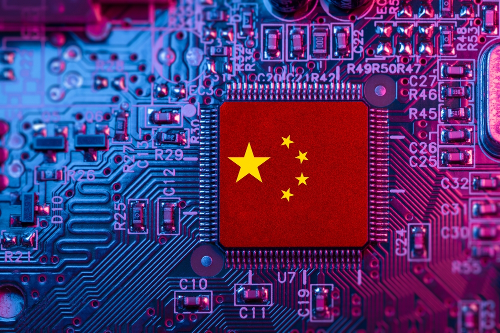
Image: Quality Stock Arts/Shutterstock